In the realm of high-performance imaging systems, the process of converting the subtle analog charge from a Charge-Coupled Device (CCD) into a pristine digital signal is a critical and complex task. The **AD9840AJSTZ from Analog Devices stands as a specialized CCD Signal Processor** designed to master this very function. This integrated circuit (IC) consolidates the entire signal chain required for CCD output, making it a cornerstone component in professional digital cameras, scientific instruments, and high-end scanners.
Architecturally, the AD9840AJSTZ is engineered to handle the low-level output of a CCD sensor with precision and care. Its signal path begins with a **low-noise Correlated Double Sampler (CDS)**. This circuit is paramount because it simultaneously samples the reference and video signal levels from the CCD pixel output. By subtracting these values, the CDS effectively cancels out common-mode noise, including reset noise (kTC noise), which is a significant source of degradation in image quality. This process is fundamental to extracting the purest possible representation of the pixel's charge.
Following the CDS, the signal is passed to a **Programmable Gain Amplifier (PGA)**. This stage provides user-adjustable gain, allowing the system to adapt to various CCD output levels and optimize the dynamic range for the subsequent Analog-to-Digital Converter (ADC). The amplified signal is then directed to a high-performance **12-bit Analog-to-Digital Converter (ADC)**. This ADC digitizes the analog waveform at high speeds, ensuring accurate digital representation of the image data. The inclusion of an internal voltage reference generator enhances stability and minimizes the need for external components.

A key feature that underscores the versatility of the AD9840AJSTZ is its **programmable offset DAC**. This allows system designers to adjust the black level of the image, ensuring that the digital output utilizes the full dynamic range of the ADC. Furthermore, the device operates on a single +5V supply, simplifying power management design. Its digital interface is designed for seamless connection with modern processors and FPGAs, outputting 12-bit data in binary or two's complement format.
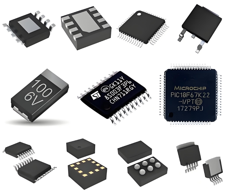
The device's programmability is managed via a serial interface, through which various parameters like gain, offset, and clock timing can be configured. This flexibility makes it suitable for a wide array of CCD sensors with differing characteristics. Its 48-lead LQFP package offers a compact form factor suitable for space-constrained designs.
In application, the AD9840AJSTZ provides a complete, single-chip imaging signal path solution. It significantly reduces design complexity, component count, and board space while delivering the high performance necessary for demanding imaging applications. Its robust design ensures excellent signal integrity from the analog sensor to the digital domain.
**ICGOOODFIND**: The AD9840AJSTZ is a highly integrated, precision CCD signal processor that excels in **noise reduction through CDS**, offers excellent **signal conditioning flexibility**, and delivers high-fidelity **12-bit digitization**. It remains a testament to Analog Devices' expertise in data conversion and analog signal processing for high-end imaging systems.
**Keywords**: CCD Signal Processor, Correlated Double Sampler (CDS), Programmable Gain Amplifier (PGA), 12-bit ADC, Analog-to-Digital Conversion.
